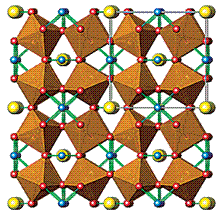
A first objective will be the development of multifunctional bulk materials with superior performances. Bulk properties will be improved during the project firstly by optimisation of the synthesis of pure CCTO strongly reducing impurities and anomalies. Then, doped CCTO will be investigated to develop new materials with improved performances. At the same time a theoretical approach will be used to build the new materials. They will be investigated regarding to all their properties with particular regard to dielectric, magnetic, ferroelectric or optical behaviour. Finally, CCTO-based phases, composites and related perovskite-based materials with high k as potential ‘next generation’ high k and/or multi-functional materials for electronic applications will be explored.
A second objective will be the thin film deposition obtained by physical methods like laser ablation and sputtering.
A third objective is to develop deposition processes for CCTO by metal organic chemical vapour deposition (MOCVD). As a further breakthrough, new equipment will be developed within the project for laser assisted Chemical Beam Epitaxy (CBE), which uses a laser to change in situ, during the deposition, the CCTO composition. The advantage of this approach is the easily scalability to large surfaces for industrial processes and the possibility to laser irradiate the film during the growth for the properties modification.
A fourth objective will be the full characterisation of all the new material properties (dielectric, but also magnetic, ferroelectric, optics).
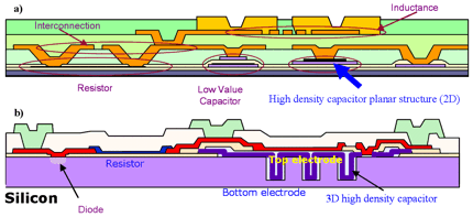
A fifth objective will be the fabrication of condensers and antennas (figure 2) to measure dielectric characteristics considering capacitive density, stability in frequency. Other devices will be developed to measure different physical properties.